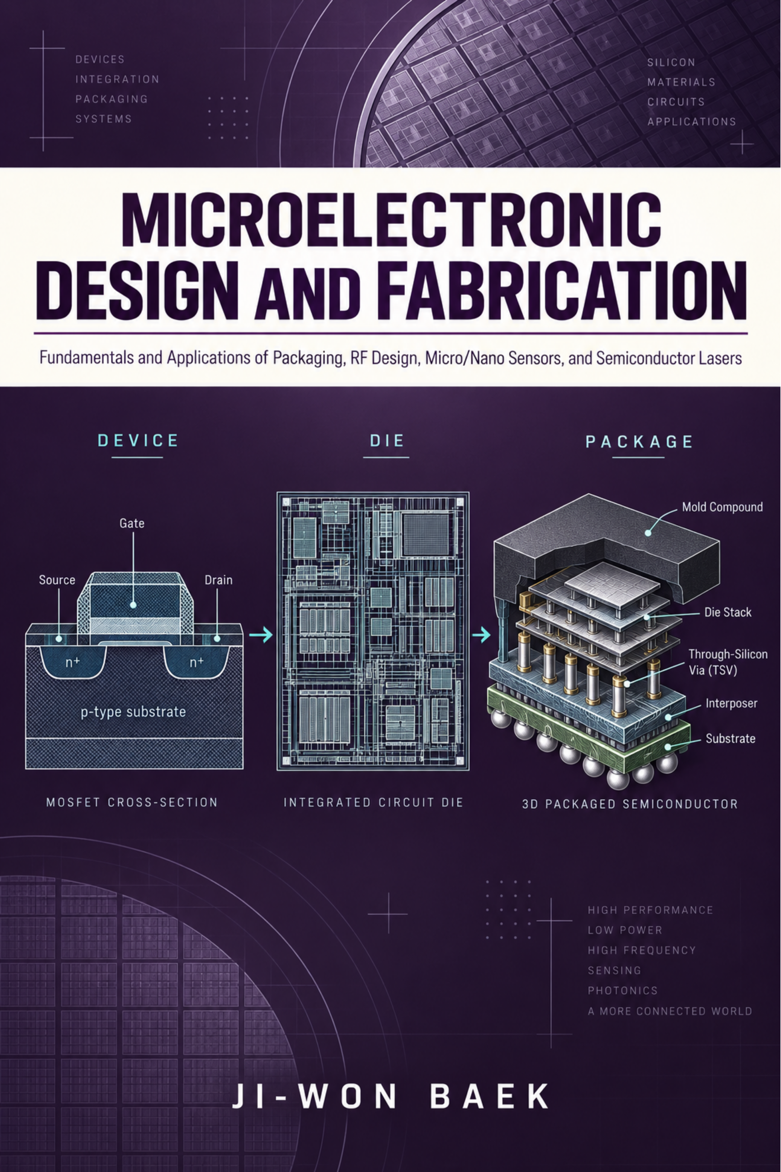
Microelectronic Design and Fabrication
Fundamentals and Applications of Packaging, RF Design, Micro/Nano Sensors, and Semiconductor Lasers
by Ji-Won Baek
A transistor model is only as good as the process that made the device.
Most books split microelectronics into separate worlds: circuit design on one side, fabrication and packaging on the other. This book keeps them in the same conversation. You begin with carrier physics and junction behaviour, build bipolar and MOSFET models from that foundation, and then design single-stage amplifiers, differential pairs, current mirrors and compensated op-amps, with feedback stability and noise treated properly rather than as an afterthought. CMOS digital chapters cover delay, power and standard cells, so the analog and digital paths stay connected.
From there you follow the wafer. Lithography, etch, implant, deposition and planarisation are presented alongside the design decisions they constrain: layout matching, electrostatic discharge protection, parasitic extraction and yield. Packaging is covered from wire bond to through-silicon vias and thermal paths, because a device that cannot be cooled or connected is not a finished product. Radio frequency chapters cover matching, scattering parameters, amplifiers, mixers and oscillators, and later chapters extend the same discipline to micromachined sensors, semiconductor lasers, and test and reliability. The result is a single arc from physics to a working, packaged, characterised part.
What you will learn:
- Semiconductor physics for designers: carriers, junctions and the behaviour that device models must capture
- Diode and bipolar transistor operation, and MOSFET models used in real design work
- Single-stage amplifiers, differential pairs, current mirrors and compensated op-amps
- Frequency response, feedback stability and noise analysis
- CMOS digital circuits: delay, power and standard cells
- Fabrication processes: lithography, etch, implant, deposition and planarisation
- Layout, design rules, matching, ESD protection, parasitic extraction and yield
- Packaging and three-dimensional integration, from wire bond to through-silicon vias and thermal paths
- RF and microwave design, micro and nano sensors, optoelectronic devices, and test, characterisation and reliability
For graduate students and engineers moving into device and integration work, this book is written for readers who need to reason across the whole chain rather than specialise in one link. If you design circuits and want to understand the process that limits them, or you work in fabrication and packaging and want to know what the circuit demands, the material is arranged to meet you where you are and carry you toward integration-level judgement.